How To Develop A PlayStation 4 Emulator(2)
Overview
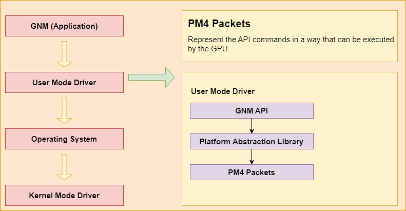
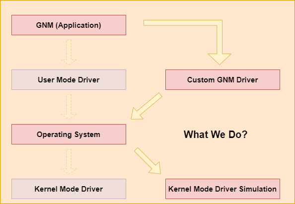
AMD Graphics driver has four levels. The first level is GNM application level. This level is implemented by the game engine or the game developer. After that, the user mode driver translates the GNM API into PM4 packets. PM4 packets represent API commands in a way that GPUs can execute. The user mode driver library is PS4’s built-in library. We have implemented a custom GNM driver to replace the built-in library. Then, Operating System gets the prepared command buffer from the user mode driver. Hands it over to the kernel mode driver. Finally, the kernel mode driver uses a ring buffer to communicate with the GPU. We implemented a command processor to process PM4 packets in order to simulate the kernel mode driver.
Our command processor is designed to simulate setting GPU registers. These GPU registers include user data registers, blend state registers, depth state registers etc. And we have implemented an AMD ISA converter to parse AMD ISA and translate it into Spirv. Finally, with these GPU registers and spirv have been prepared, we translate them into Vulkan API and rendering the game.
Graphics Libraries
Graphics Driver Overview
AMD Graphics driver has four levels. The first level is GNM application level. This level is implemented by the game engine or the game developer. Game developers call these GNM commands to prepare GPU resources, such as buffer, PSO and draw commands.
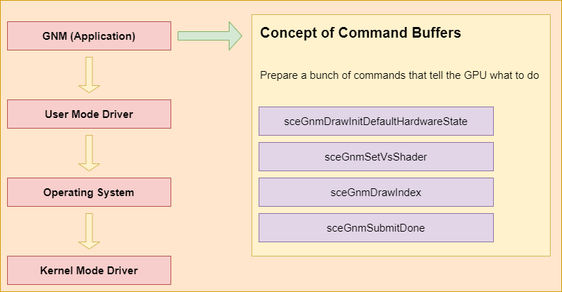
After that, the user mode driver translates the GNM API into PM4 packets. PM4 packets represent API commands in a way that GPUs can execute. The translation library is called the Platform Abstraction Library (Linux driver is open source on Github). It translates the Graphics APIs (Vulkan/GNM) into PM4 packets. PAL is a shared component that is designed to encapsulate certain hardware and OS-specific programming details for many of AMD’s 3D and compute drivers.
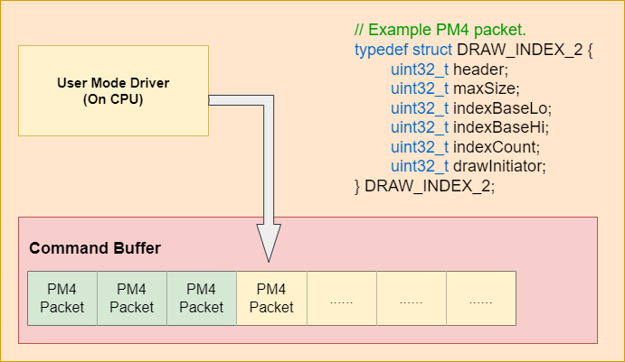
Here is a PM4 example. The header member is the opcode of draw index 2. The indexBaseLo and indexBaseHi are the lower and higher part of the GPU address. As we mentioned above, the GPU memory and the CPU memory are viewed as the same in our emulator, which means that we can get the resource from the allocated memory. The user mode driver will generate the PM4 packets and write them to the command buffer.
Then, Operating System gets the prepared command buffer from the user mode driver. Hands it over to the kernel mode driver. Ensure that the user mode driver cannot hang the whole system.
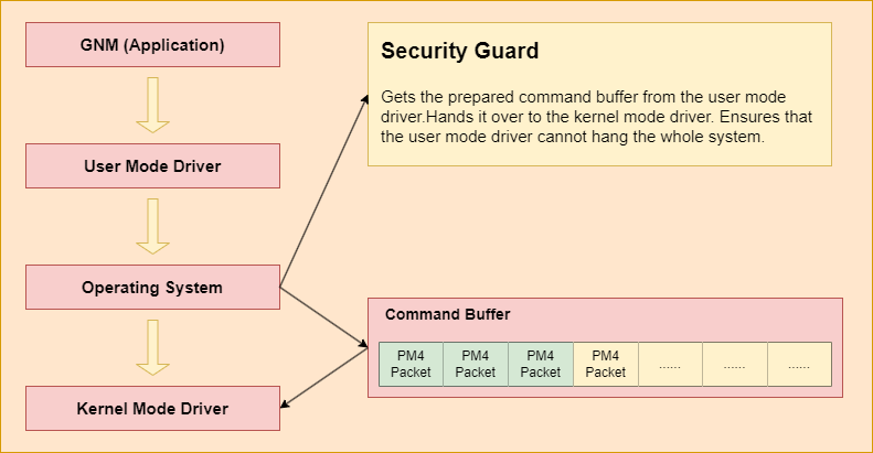
Finally, the kernel mode driver uses a ring buffer to communicate with the GPU. It contains addresses to command buffers. CPU increments the write pointer. GPU increments the read pointer.
There are two steps that we should do. The first step is to implement a custom GNM driver that translates the GNM API into PM4 packets. The second step is to implement a kernel mode driver to simulate register setting. The GNM driver and the kernel mode driver are running on the CPU. We also need to implement a command processor to process PM4 packets and translate them into the Vulkan API. The command processor runs on the GPU, which is different from the driver.
GNM Driver
Here is an example of the GNM API implementation. As you can see, it is non-human-readable. You can’t understand these magic hexadecimal numbers without AMD’s official documentation.
1 | |
Since the PM4 packets generated from the GNM driver are used in the kernel mode driver, which is also under our control. It means we can add a custom more human-readable format. This format is encoded in the GNM driver and decoded in the kernel mode driver.
We generate the OPcode by the PM4_HEADER_BUILD macro. The custom OPcode is marked as IT_OP_CUS.
1 | |
We process the custom OPcode separately in the kernel mode driver for the IT_OP_CUS case.
1 | |
Here is the implementation of the GNM DrawIndex API. We generate the custom PM4 packets and output the result to the command buffer.
1 | |
Kernel Mode Driver
In the kernel mode driver, we decode the PM4 packets from the command buffer and set registers based on the decoded packets.
1 | |
Three types of PM4 command packets are currently defined. They are types 0, 2 and 3. We only parse the PM4 packets with the PM4_TYPE_3 type.
1 | |
A PM4 command packet consists of a packet header, identified by field HEADER, and an information body, identified by IT_BODY, that follows the header. The packet header defines the operations to be carried out by the PM4 micro-engine, and the information body contains the data to be used by the engine in carrying out the operation. Following parts are the packets we will process.
Constant Engine Packets
DUMP_CONST_RAM: Sent only to the Constant Engine to instruct the CE to move data from one or more RAM slot lines to L2 Memory.
INDIRECT_BUFFER_CONST: This packet is used for dispatching Constant Indirect Buffers, new in SI. A separate constant buffer allows the CP to process constants ahead of and concurrently with the “draw command buffer”
SET_CONTEXT_REG
SET_CONTEXT_REG: This packet loads the eight-context-renders tate register data, which is embedded in the packet, into the chip.
The REG_OFFSET field is a DWord-offset from the starting address:
1 | |
All the render state data in the packet is written to consecutive register addresses beginning at the starting address. The starting address for register data is computed as follows:
1 | |
Many render states are related to SET_CONTEXT_REG. It includes the following states:
render target states:
1 | |
PA(Primitive Assembler), SC(Scan Converter) modes control:
1 | |
Here is the PA_SU_SC_MODE_CNTL structure:
1 | |
PA(Primitive Assembler)
Primitive Assembler accumulates vertices that span a triangle and forwards triangles to SC.
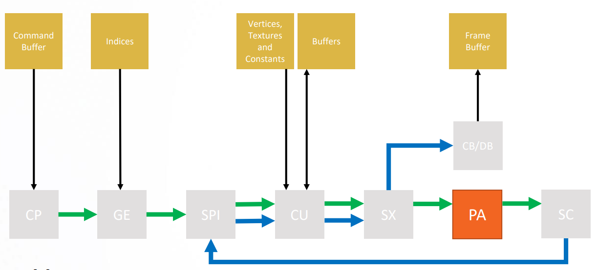
Primitive Assembly is the stage in the OpenGL rendering pipeline where Primitives are divided into a sequence of individual base primitives. The purpose of the primitive assembly step is to convert a vertex stream into a sequence of base primitives. For example, a primitive which is a line list of 12 vertices needs to generate 11 line base primitives. The order in which primitives are processed is well-defined (in most cases).
SC(Scan Converter)
Scan Converter determines pixels covered by each triangle and forwards them to SPI.
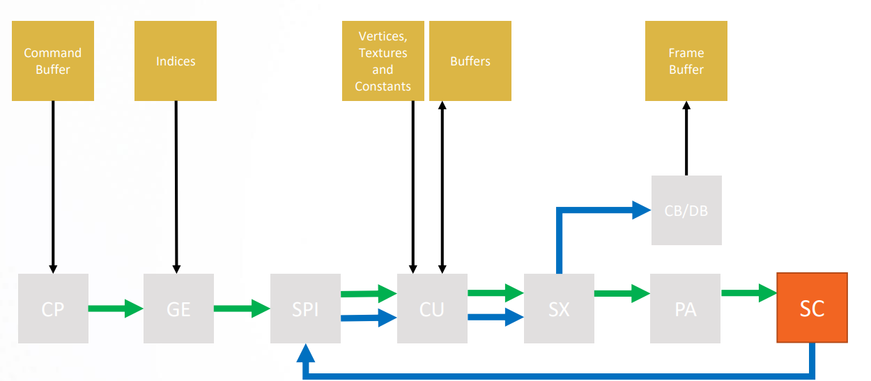
Scan conversion generates the set of fragments corresponding to each primitive. Each fragment contains window coordinates x, y, and z, a color value, and texture coordinates. The fragment values are generated by interpolating the attributes provided at each vertex in the primitive. Scan conversion is computationally intensive since multiple attribute values must be computed for each fragment. During scan conversion the generated fragments are also tested against the scissor rectangle, and fragments outside the rectangle are discarded
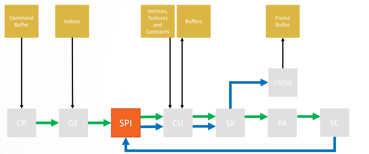
SPI(Shader Processor Input)
Shader Processor Input accumulates work items and Sends them in waves to the CU.
1 | |
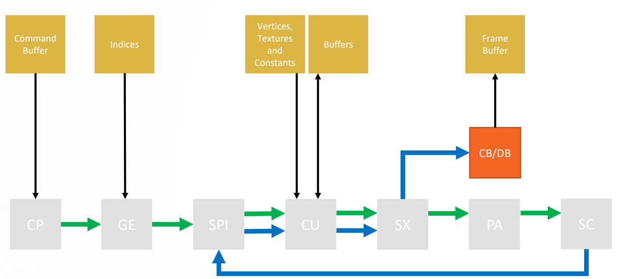
CB/DB(Color Backend/Depth Backend)
Depth Backend discards occluded fragments based on depth / stencil. Color Backend write colored fragments to render targets.
1 | |
SET_SH_REG
This packet updates the shader persistent register state in the SPI, which is embedded in the packet, into the chip. The starting address for register data is computed as follows:
1 | |
SET_SH_REG is used to set the shader user data. For each shader type, there are 16 user data hardware registers (e.g., SPI_SHADER_USER_DATA_PS_0-15). These 16 32-bit values are the only interface through which the driver can specify SRDs to the shader:
These registers are written with SET_SH_REG PM4 commands in the driver’s indirect buffer.
At shader launch, SPI loads values from these 16 hardware registers into SGPRs 0 - 15 to be read by the shader. The actual number of values loaded by SPI is controlled by the USER_SGPR field in the SPI_SHADER_PGM_RSRC2_xx register.
1 | |
Draw Related Packets: Graphics Ring
INDEX_TYPE: Set the index buffer format.
1 | |
There are three optional index formats: 16 bit, 32 bit and 8 bit index formats.
1 | |
NUM_INSTANCES: NUM_INSTANCES is used to specify the number of instances for the subsequent draw command.
1 | |
Custom PM4 Packets
As we mentioned in the GNM driver part, we added a custom PM4 packet format to the GNM API. The opcode of these packets is IT_OP_CUS. We process these packets separately.
1 | |
The vertex shader input and pixel shader input are set by custom PM4 packets. We will detail its usage latter.
1 | |
GPU Translator
After all registers have been set, we can implement a GPU translator that translates GPU registers into Vulkan API.
Shader Binary Code Layout
The shader binary code we obtained from the game project is represented in AMD ISA format. It is compiled from PSSL (Play Station Shading Language). Here is the shader binary code layout for PS4.
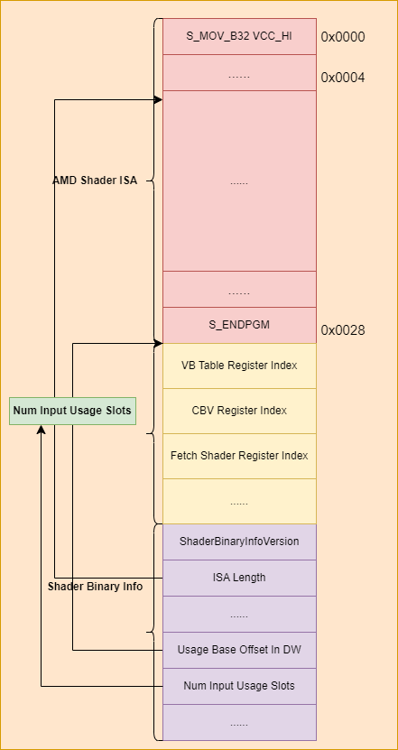
The shader binary code is starts with the AMD ISA compiled from the PSSL. Following the ISA are the shader usage slots that point to the user data register. We will detail it later. The shader binary information is after shader usage slots. It is an exclusive part for PS4. It contains information about the shader binary code, such as the ISA length, the shader usage slots offset relative to the shader binary information address.
AMD ISA Parser and Translator
Since the game is rendered using Vulkan, we must translate the AMD ISA into Spirv. Fortunatly, there are many open source tools that can disassemble the AMD ISA, such as the Radeon GPU Analyzer. In PSET4, we rely on the ISA translator developed by FPCS4. The reason we use this translator is that it can converts the ISA into Spirv directly.
Due to the fact that the FPCS4’s ISA translator requires some additional information contained within the ISA, we need to implement a simplified ISA parser in order to obtain these details. What’s more, the parsed information is also used in the resource binding.
AMD ISA has six types of operation: scalar ALU operations, vector ALU operations, scalar memory operations, vector memory operations, flat memory instructions and data share operations. We take the scalar ALU operation as an example to introduce the instruction format.
Scalar ALU (SALU) instructions operate on a single value per wavefront. These operations consist of 32-bit integer arithmetic and 32- or 64-bit bit-wise operations. The SALU also can perform operations directly on the Program Counter, allowing the program to create a call stack in SGPRs. Many operations also set the Scalar Condition Code bit (SCC) to indicate the result of a comparison, a carry-out, or whether the instruction result was zero.
SALU instructions are encoded in one of five microcode formats, shown below:
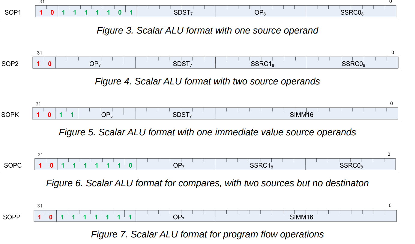
Each of these instruction formats uses some of these fields:
| Field | Description |
|---|---|
| OP | Opcode: instruction to be executed. |
| SDST | Destination SGPR. |
| SSRC0 | First source operand. |
| SSRC1 | Second source operand. |
| SIMM16 | Signed immediate 16-bit integer constant. |
The instructions begin with two or more bits that are used to determine which instruction the uint32 value belongs to. For example, the SOP1 instruction begins with 1011 1110 1, which is 0xbe800000 in hexadecimal format.
1 | |
We get the value of the first 9 bits by SQ_ENC_SOP1_MASK and compare it with SQ_ENC_SOP1_BITS. If the compare result is true, we can process this instruction as the SOP1 instruction.
1 | |
Here is an example:
1 | |
Vertex Shader State
The shader binary code contains shader usage slots. It stores the index that point to the user data reigisters. Each shader type has 16 user data registers. The content of the user data registers depends on the shader usage slot type. Generally, it stores the resource descriptor address of the shader input resources. The resource descriptor contains resource information such as the resource GPU address, resource format and stride.
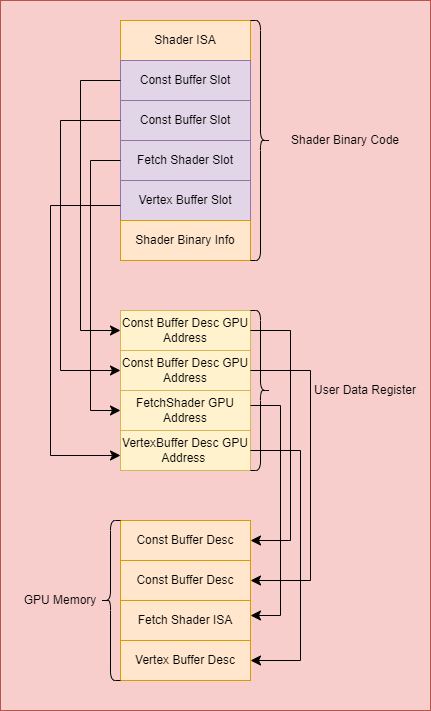
The first step is to get the shader register index from the shader binary code for the resources used by the vertex shader. The base address of the shader usage slot is calculated based on shader binary information.
1 | |
Set Vertex Shader Constant Buffer
The constant buffer usage type is kShaderInputUsageImmConstBuffer. We can get the user data register index by the GetUsageRegisterIndex function.
1 | |
Then, retrieve the constant buffer resource descriptor’s GPU address from the user data register.
1 | |
The shader buffer resource descriptor has four words. The first word stores the lower part of the buffer’s byte base address.
1 | |
The second word has four members:BASE_ADDRESS_HI: The higher part of the buffer byte base address.STRIDE: Stride, in bytes. [0..2048]CACHE_SWIZZLE : buffer access. optionally swizzle TC L1 cache banks.SWIZZLE_ENABLE: Cache Swizzle Array-Of-Structures according to stride, index_stride and element_size; else linear.
1 | |
The third word stores the number of records in a buffer. Each record is STRIDE bytes. We will detail the last word later.
1 | |
The buffer’s GPU address is calculated from word0 and word1.
1 | |
We calculate the buffer size by multiplying the element stride and the number of the elements.
1 | |
The constant buffer can now be created and set now that all the resources needed have been prepared.
1 | |
Vertex Attributes And AMD GCN Assembly
We should get the vertex attributes information before setting the vertex buffer. The vertex attributes are obtained from the fetch shader. Here is an example of the fetch shader ISA. The fetch shader is used to load the vertex element from the vertex buffer, which means that we can obtain the vertex attributes by parsing shader ISA.
1 | |
In this example, the hardware loads the buffer address into scalar registers 8 - 19 from scalar registers 2 - 3 by the ‘s_load_dwordx4’ instruction. The registers 2 - 3 are set before wavefront execution. Prior to start of every wavefront execution, CP/SPI sets up the register state based on enable_sgpr_* and enable_vgpr_* flags in amd_kernel_code_t object:
SGPRs before the Work-Group Ids are set by CP using the 16 User Data registers.
SGPR register numbers used for enabled registers are dense starting at SGPR0: the first enabled register is SGPR0, the next enabled register is SGPR1 etc.; disabled registers do not have an SGPR number. Because of hardware constraints, the initial SGPRs comprise up to 16 User SRGPs that are set up by CP and apply to all waves of the grid. It is possible to specify more than 16 User SGPRs using the enable_sgpr_* bit fields, in which case only the first 16 are actually initialized. These are then immediately followed by the System SGPRs that are set up by ADC/SPI and can have different values for each wave of the grid dispatch.
In this example, we load the buffer address from the user data registers 2 and 3.
1 | |
After that, we load the per-vertex data from the buffer based on the address stored in registers 8 - 19. Which position the current thread should to loaded from the buffer is determined by the v0. VGPR register numbers used for enabled registers are dense starting at VGPR0: the first enabled register is VGPR0, the next enabled register is VGPR1 etc.; disabled registers do not have a VGPR number. VGPR v0 is always initialized with a work-item ID in the x dimension (in commpute shader). Registers v1 and v2 can be initialized with work-item IDs in the y and z dimensions, respectively.
In the vertex shader, v0 is intialized with the vertex index. The number of the buffer_load_format instruction is 3, which means that the vertex shader has 3 vertex attributes.
The fetch shader is not part of the vertex shader. It is stored separately. The GPU address of the fetch shader can be obtained from the user data registers.
1 | |
Vertex Buffer And Vertex Layout
The vertex buffer is the same as the constant buffer mentioned above. We can get the GPU address from the buffer descriptor, which is the same as the constant buffer. Unlike the constant buffer, the vertex buffer needs the format information, while the constant buffer doesn’t need these. The buffer format is specified in the fourth word of the buffer resource descriptor. Here is the member layout of the word3.
1 | |
The BUF_NUM_FORMAT and BUF_DATA_FORMAT specifies data and numeric formats used by the operation. The default numeric format is BUF_NUM_FORMAT_UNORM. The default data format is BUF_DATA_FORMAT_8.
1 | |
Supported data formats are defined in the following structure:
1 | |
Supported numeric formats are defined below:
1 | |
After the data formats and numeric formats have been prepared, we can translate them into VKFormat. For example, BUF_NUM_FORMAT_UNORM and BUF_DATA_FORMAT_8 correspond to VK_FORMAT_R8_UNORM format.
1 | |
Texture Tiling And Detile
The image resource descriptor is obtained from the user data register, which is the same as the buffer resource.
1 | |
The naive view of an image in memory is that the pixels are stored one after another in memory usually in an X-major order. An image that is arranged in this way is called “linear”. Linear images, while easy to reason about, can have very bad cache locality. Graphics operations tend to act on pixels that are close together in 2-D euclidean space. If you move one pixel to the right or left in a linear image, you only move a few bytes to one side or the other in memory. However, if you move one pixel up or down you can end up kilobytes or even megabytes away. Tiling (sometimes referred to as swizzling) is a method of re-arranging the pixels of a surface so that pixels which are close in 2-D euclidean space are likely to be close in memory.
We should convert the tiled format texture into a linear format texture before using it.
While any non-linear representation is typically referred to as “tiling”, some hardware implementations actually use a more complex layout in order to provide further locality of reference. One such scheme is Morton order:
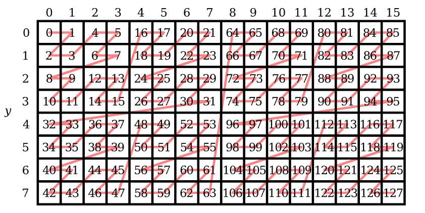
The following code shows how to convert the linear xy index into an element index.
1 | |
For each pixel, we calculate the morton code offset and fetch the pixel data from the tiled image buffer. Then, we can get an image stored in linear format.
1 | |
Pipeline State And Draw Index
After all resources and GPU registers have been prepared, we can finally set the pipeline state.
The depth stencil states are obtained from the DEPTH_CONTROL register.
The render target states are obtained from the RENDER_TARGET register.
The color blend state is obtained from the CB_COLOR_CONTROL register.
1 | |
1 | |
We translate these registers into the Vulkan state and set the graphics pipeline state.
1 | |
When we process the draw index PM4 packet (OP_CUS_DRAW_INDEX), we set the pipeline state, get the index buffer from the PM4 packet and execute the Vulkan draw index command.
1 | |
1 | |
rendering result in loading stage: